Spartan-3E FPGA Design Guide for prototyping and

PCB. This guide is based on Xilinx FPGA Spartan-3E, but designers of the other FPGA types can also follow this design flow, by respecting design requirement
Learn MoreKeyboard pcb design guide - ycmxdz.hollywoodmac.shop
Mijing T23 Triaxial Multifunction PCB Board Holder Fixture, snatcher. Meet Adam Silver's Form Design Patterns, a practical guide to designing and building forms for the web. take a look at the list available on the Keyswitch guide at the Mechanical Keyboards store. The ErgoDox EZ is an ergonomic split design keyboard with a fully programmable PCB and hotswap PCB.
Learn MoreXilinx pcb design guide Jobs, Employment | Freelancer
Search for jobs related to Xilinx pcb design guide or hire on the world's largest freelancing marketplace with 20m+ jobs. It's free to sign up and bid on jobs.
Learn MoreXilinx/Cadence PCB Guide (UG629
2022. 5. 5. · Xilinx/Cadence PCB Guide (UG629) Author: Xilinx, Inc. Subject: Discusses processes and mechanisms available in the ISE Design Suite and various Cadence tools to eff iciently implement an FPGA on a PCB Keywords: pcb,design,cadence,printed circuit board,fpga,schematic,symbol,design flow,layout Created Date: 6/17/ 4:10:32 PM
Learn MoreSpartan-6 FPGA PCB Design and Pin Planning Guide
Text of Xilinx UG393 Spartan-6 FPGA PCB Design Guide FPGA PCB Design and Pin Planning UG393 (v1.3) October · Spartan-6 FPGA PCB Design and Pin Planning Guide.
Learn MorePDF Xilinx UG393 Spartan-6 FPGA PCB Design Guide - Qi-HardwarePDF
Spartan-6 FPGA PCB Design Guide www.xilinx.com5 UG393 (v1.0) September 21, Preface About This Guide This guide provides information on PCB design for Spartan®-6 devices, with a focus on strategies for making design decisions at the PCB and interface level. Guide Contents
Learn MoreHardware Design Guide - Opal Kelly Documentation Portal
Details on the available standards can be found in the following Xilinx documentation: Zynq UltraScale+ MPSoC Data Sheet: DC and AC Switching Characteristics (
Learn MoreXilinx ug393 spartan 6 fpga pcb design guide | PDF4PRO
Spartan-6 FPGA PCB Design and Pin Planning www.xilinx.com UG393 (v1.3) October 17, Xilinx is disclosing this user guide, manual, release note,
Learn MoreThe Ultimate Guide to Choosing Xilinx XC2C64A-5VQ44C
A Complex Programmable Gate Array (CPLD), which Xilinx XC2C64A-5VQ44C is one a quotation from RayPCB to get an idea of the cost of designing the Complex
Learn More7 Series FPGAs PCB Design Guide (UG483) - Xilinx
2022. 5. 5. · 7 Series FPGAs PCB Design Guide www.xilinx.com UG483 (v1.14) May 21, 01/10/ 1.12 Updated introductory paragraph in About This Guide. Changed “100 MHz” to
Learn MorePCB Design Considerations for FPGA Accelerator Cards
fabrication technology used in the PCB design process. Component Placement Guidelines Target Device: Xilinx® Virtex® UltraScale+™ FPGA.
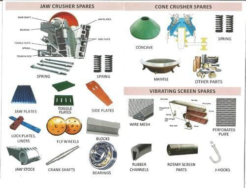
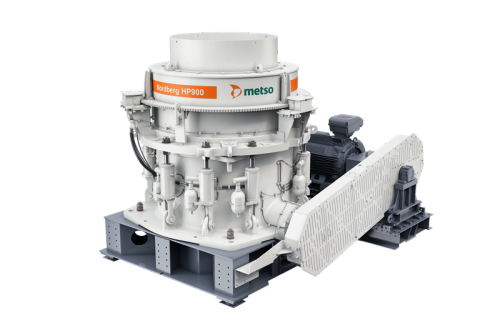
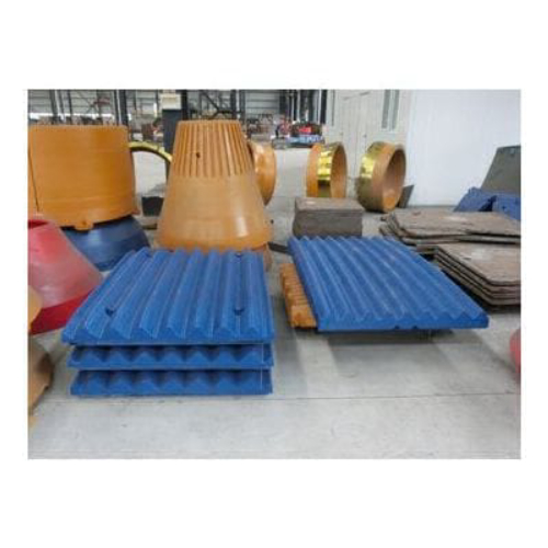
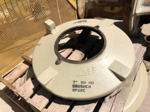
Learn MoreC95 DAMPER C-SERIE, PU 90 SHA xilinx pcb design guide
mill copper parts america xilinx schematic review checklist side plate for jaw crusher crusher centrifugal casting traders zambia used rock crushers for sale. C95 jaw crusher parts list. 580274, SENSOR INST C95, C106, 953615, DAMPER C-SERIE, PU 90 SHA. 932734, BRACKET C95, C125, C140, C145, C160, 705401331855, V-RING SEAL TSN 518 A.
Learn MoreCSG325 PCB Design Rules - Xilinx
CSG325 PCB Design Rules. Hello, I seek layout information for the CSG325 0.8mm pitch BGA package. I would like to find recommendations similar to those found in UG112 pages 87 and 88 with listed pad size, solder mask opening, via pad size, etc. Is there a similar document for the chip scale packages like the CSG325? Pete. General Discussion. Like.
Learn MoreVersal ACAP PCB Design User Guide (UG863) - Xilinx

2022. 6. 15. · Versal ACAP PCB Design User Guide (UG863) Document ID. UG863. Release Date. 2022-06-15. Revision. 1.4 English. Overview. Introduction to Versal ACAP.
Learn MoreXilinx UG393 Spartan-6 FPGA PCB Design Guide - Qi-Hardware

2010. 1. 27. · 6 www.xilinx.com Spartan-6 FPGA PCB Design Guide UG393 (v1.0) September 21, Preface: About This Guide This all-encompassing configuration guide includes chapters on configuration interfaces (serial and parallel), multi-bitstream management, bitstream encryption, boundary-scan and JTAG configuration, and reconfiguration techniques.
Learn Morethe newest generation of
the newest generation of Xilinx FPGAs. This application note is a condensed version of the best practices for configuration of Platform Flash PROMs and serves as a guide for a basic configuration setup. The focus of this document is on Spartan™-3A FPGAs. Platform Flash PROMs. UG1410 (v1.0) July 8, www.xilinx.com ZCU208 Board User Guide 2 Se n d Fe e d
Learn MoreZynq-7000 User Guide Datasheet by Xilinx Inc.

Zynq-7000 PCB Design Guide www.xilinx.com 3. UG933 (v1.13.1) March 14, 2019. 12/04/ 1.6 Changed “DDR3” to “DDR3/3L” throughout document.
Learn MoreUltraScale+ FPGAs Product Tables and Product Selection Guide

Please contact your Xilinx representative for the latest information. See UG583, UltraScale Architecture PCB Design User Guide for important migration
Learn MorePcb Design Checklist - Virtex UltraScale+ FPGAs - ManualsLib
Pcb Design Checklist - Xilinx Virtex UltraScale+ FPGAs User Manual Decoupling capacitors should be provided on the PCB near the GTM transceiver power pins.
Learn MorePDF Zynq-7000 SoC PCB Design Guide - XilinxPDF
This guide provides information on PCB design for the Zynq®-7000 SoC, with a focus on strategies for making design decisions at the PCB and interface level. This Zynq-7000 SoC PCB Design Guide, part of an overall set of documentation on the Zynq-7000 SoC, is available on the Xilinx website at www.xilinx.com/zynq. Additional Support Resources
Learn MoreFirst-Time-Right Circuit Board Design: 4 Tips From the Experts
Just recently we completed a High-density Interconnect (HDI) PCB design based on a Xilinx Virtex-7 FPGA with numerous 933MHz DDR3 memory buses, multiple PCI
Learn MoreDocumentation Portal - Xilinx

Loading Application // Documentation Portal . Resources Developer Site; Xilinx Wiki; Xilinx Github; Support Support Community
Learn More7 Series FPGAs PCB Design Guide (UG483
Xilinx assumes no obligation to correct any errors contained in the Materials, or to advise you of any corrections or update. You may not.
Learn MorePDF UltraScale Architecture PCB Design - xilinx.eetrend.comPDF
This chapter documents the power distribution system (PDS) for UltraScale devices, including decoupling capacitor selection, placement, and PCB geometries. A simple decoupling method is provided fo r each device. Basic PDS design principles are covered, as well as simulation and analysis methods.
Learn MoreZynq UltraScale+ MPSoC Design Overview - Xilinx
UG1169 - Xilinx Quick Emulator: User Guide: 03/26/ UG1186 - Libmetal and OpenAMP for Zynq Devices User Guide: 06/30/ : UltraScale and UltraScale+ User Guides UG583 - UltraScale Architecture PCB Design Guide: 06/03/ : Support Resources. Support Resources. Design Advisories Date
Learn MorePDF 7 Series FPGAs PCB Design Guide (UG483) - Rice UniversityPDF
UG483 (v1.13) August 18, www.xilinx.com 7 Series FPGAs PCB Design Guide 02/12/ 1.6 Updated first paragraph of Recommended PCB Capacitors per Device. Added Fixed Package Capacitors per Device . In Table 2-2, removed XC7A350T and added XC7A200T (SBG484). In Table 2-4, removed XC7V1500T and corrected packages for XC7VX1140T from FFG to FLG.
Learn MoreXilinx UG393 Spartan-6 FPGA PCB Design Guide
2022. 5. 5. · PCB Design and Pin Planning Guide UG393 (v1.3) October 17, 2012. Spartan-6 FPGA PCB Design and Pin Planning www.xilinx.com UG393 (v1.3) October 17, Xilinx is disclosing this user guide, manual, release note, and/ or specification (the "Documentation") to you solely for use in the development
Learn MoreHigh-Speed PCB Design Considerations - Lattice Semi
lines that are run through a backplane. These aspects include PCB line structure, vias, device packaging and backplane connectors. A PCB design checklist is provided to aid the designer. Some frequency specific discussion and guidelines are given. This document also discusses Lattice Semiconductor's FPGA product line and its SerDes high-speed
Learn MoreXilinx 7 Series Design Guide
Overview This is in no way meant to replace the comprehensive Xilinx design guides for 7 Series devices, but rather serve as a quick
Learn MorePDF 7 Series FPGAs PCB Design Guide (UG483) - china.origin.xilinx.comPDF
7 Series FPGAs PCB Design Guide www.xilinx.com UG483 (v1.14) May 21, The information disclosed to you hereunder (the "Materials") is provided solely for the selecti on and use of Xilinx products. T o the maximum extent permitted by applicable law: (1) Materials are made availa ble "AS IS" and with all faults, Xilinx hereby DISCLAIMS ALL
Learn MorePCB Design Checklist
2022. 7. 27. · Table: PCB Design Checklist for PS-GTR is a checklist of items that can be used to design and review any Zynq UltraScale+ MPSoC PS-GTR transceiver schematic and layout.
Learn More
Leave A Reply